14 February 2022
H2020 Project ELENA
The ELENA project promises to benefit the entire photonics sector by developing the first European lithium niobate on insulator (LNOI)-based platform for photonic integrated circuits (PICs) and establ...
Combining CSEM’s ultra-low-power ASIC design experience with the Extreme-Low Power (ELP) DDC technology from MIFS enables new world records in power consumption. A complete process design kit, along with a range of mixed-signal silicon IPs, is now available.

The phenomenal growth of the Internet of Things and wearable technologies, combined with edge processing, is placing ever-greater demands on low-power electronics. Smart dust and unobtrusive wearables require tiny batteries or even self-powering, harvesting energy from their surroundings.

CSEM, a leader in ultra-low-power ASIC design, and Mie Fujitsu Semiconductor (MIFS), a leading wafer foundry, have joined forces to develop a near-threshold 0.5V ecosystem; since energy scales with the square of the supply voltage, huge reductions in energy consumption can be achieved for similar performance. MIFS’ Deeply Depleted Channel (DDC) technology is perfectly adapted to low-power applications, while its immunity to random dopant fluctuations makes it suitable for low-voltage operation. Low-voltage operation, however, is still subject to process and temperature and other variations. To overcome the impact from these variations CSEM and MIFS applied a variety of design techniques and implemented Body-bias-based Adaptive Dynamic Frequency Scaling (ADVbbFS) as one of the key IPs.
A 32-bit RISC microcontroller designed in C55DDC was presented recently at IEEE CICC in Austin, TX, demonstrating only 2.5uW/MHz—a new world record in a 55nm CMOS process.
For Keizaburo Yoshie, Senior Vice-President, MIFS, “Combining CSEM’s ULP design experience with MIFS’ DDC process technology helps realize IOT chip designs that are unbeatable in energy efficiency.” Alain-Serge Porret, CSEM’s Vice-President, Integrated & Wireless Systems, says, “Low-voltage design is essential for the next generation of IOT devices; we were delighted to team up with MIFS to make this dream a reality.”
A complete design ecosystem is now available, including a process design kit (PDK) with all libraries and key analogue IP blocks.
You can meet CSEM and MIFS at the Sensors Expo, 26-27 June in San Jose, IoT & Wireless Pavilion, Booth #1045.
14 February 2022
The ELENA project promises to benefit the entire photonics sector by developing the first European lithium niobate on insulator (LNOI)-based platform for photonic integrated circuits (PICs) and establ...
8 February 2023
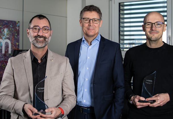
For the second year in a row, CSEM is granting its Inventor Award to a patented technological innovation with a high impact on our business, the industry and society in general. This year, the award h...

10 March 2021
CSEM has announced the two winners of its 2020 Digital Journey award: Gait Up, based in Renens in the Canton of Vaud, and Definition12, based in Reinach in the Canton of Basel-Landschaft....