First production-ready TFLN photonic foundry emerges from CSEM spin-off
- CSEM announces the incorporation of its spin-off CCRAFT in April 2025.
- CCRAFT is a new foundry manufacturing photonic integrated circuits—key components for optical communication, AI data centers, and quantum technologies.
- It is the first production-ready pure-play foundry in the world to offer chips based on Thin‑Film Lithium Niobate (TFLN) technology, one of the fastest growing platforms in photonics.
- CCRAFT already delivers pilot production today and plans to expand its production lines in Neuchâtel to deliver millions of advanced photonic chips.

The start-up CCRAFT is launched to commercialize the production of photonic chips, an essential component for next-generation telecom, AI data centers, and quantum technologies. It is the first production-ready company worldwide to sell integrated circuits based on Thin‑Film Lithium Niobate (TFLN), widely seen as the future platform for high‑performance photonics. Registered in April 2025, the company has been developing its technology at CSEM for six years. The team has been delivering photonic chips through a pre‑commercial offering at CSEM using a pilot production line for the past four years. CCRAFT plans additional manufacturing capacities in Neuchâtel to scale up production.
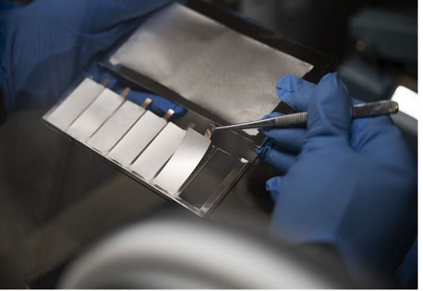
The CSEM spin-off company CCRAFT has been launched in April 2025 to manufacture next‑generation photonic integrated circuits. These advanced photonic microchips process light signals for high-speed optical communications, and high‑performance computing (HPC), and also enable innovative sensing systems and emerging quantum technologies. CCRAFT’s technology is based on thin‑film lithium niobate (TFLN), widely seen as one of the most promising technologies for photonic chips.
“Mainstream photonic platforms are hitting fundamental limits in bandwidth and energy efficiency, bottlenecks amplified by the AI-driven demand for data. TFLN is a very promising material platform capable of meeting these next-generation performance needs” says Hamed Sattari, CCRAFT Founder and CEO. “We have developed our technology over the last six years at CSEM, and manufactured thousands of photonics chips for more than 40 partners. We are now ready to scale up production.”
Combining optics and electronics: The TFLN advantage
Today’s global data communication depends on a massive network of data centers and internet exchange points connected by optical fibers, cables, and even free-space links. As data flows through these networks, it constantly needs to switch between electronic and optical signals—handled by special components like transceivers in data centers.
With the rapid growth of data, especially driven by AI, current technologies are hitting their limits in speed and energy efficiency. Some projections even suggest that data centers could soon use more than 20% of the world’s electricity. Although new architectures and faster electronic chips are being developed, the biggest challenge remains the conversion between light and electricity.
Most existing platforms, such as silicon photonics or indium phosphide (InP), cannot deliver the leap in performance the market needs. Chips, built with Thin-Film Lithium Niobate (TFLN), promise up to 8 times higher speed and consume up to 10 times less energy than conventional optical components.
Thanks to its excellent electro-optic properties and compatibility with modern chip manufacturing, TFLN enables ultra-fast and efficient data transfer and industrial adaptation. Beyond data communication, TFLN also opens new possibilities for applications in quantum technologies, advanced sensing, and space systems—thanks to its low optical losses, wide transparency range, and ability to work at standard electronics voltages.
“TFLN combines several key advantages: high electro‑optic efficiency, low optical losses, a wide transparency window, optical nonlinearities, and compatibility with microelectronic systems. This positions TFLN as a transformative platform not only for data communication, but also for quantum technologies, lidar, advanced sensing, and space applications,” explains Sattari. “CCRAFT offers both monolithic chips, built entirely on a TFLN substrate, and hybrid designs that combine TFLN with silicon for easier integration.”
First Industrial-Scale TFLN Foundry Ready to Deliver
CCRAFT also provides a dedicated Process Design Kit (PDK) that supports customers in the designing and testing of the microcircuits to be produced. The PDK contains a complete modeling of each component’s physical characteristics and performance to ensure that the manufactured chips behave as designed. The company can produce Multi‑Project Wafers (MPW) containing up to 800 different chips per wafer, which can help clients speed‑up the modelling and testing phase.
“We are the first company in the world to be production-ready for TFLN‑based chips,” Sattari highlights. “Other businesses are still raising funds or offering so-called virtual foundry services, with the need to outsource the actual production.” Sattari and his team have been producing photonics integrated circuits for six years on CSEM’s cutting‑edge foundry infrastructure. “Our tight collaboration with CSEM allows us to move from pilot manufacturing to industrial production,” states Sattari. The company plans to install additional production lines in Neuchâtel to deliver 12 million chips per year by 2030 and capture up to 30% of the worldwide market.
“CSEM provides a unique platform for CCRAFT,” notes Bahaa Roustom, VP Marketing & Business Development at CSEM: “By leveraging CSEM's infrastructure and years of know‑how and also Horizon Europe projects, CCRAFT can accelerate the time to production and could become the first company in the world offering industrial production of components essential to high-performance optical information processing. This is a real opportunity for Switzerland and Europe to regain some sovereignty in an essential communication and computing technology. The launching of CCRAFT shows the impact of CSEM’s startup program that supports innovation in a structured and ambitious way. It also aligns with our objectives to foster world-class innovation, follow tightly where the market is going, and enable Swiss high-tech companies to flourish.”


Additionnal information
CSEM
Ada Hinrichs
Head of Marketing & Communications
+41 78 658 40 42
media@csem.ch
Related Press
14 February 2022
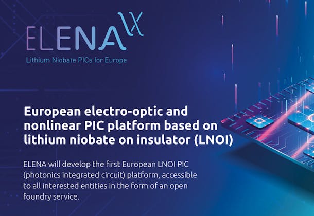
H2020 Project ELENA
The ELENA project promises to benefit the entire photonics sector by developing the first European lithium niobate on insulator (LNOI)-based platform for photonic integrated circuits (PICs) and establ...
19 September 2022
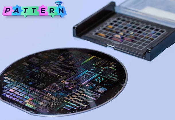
Launch of the Horizon Europe RIA project PATTERN
Next generation ultra-high speed Photonics ICs via heterogenous integration of LNOI and InP platforms....
25 February 2025
CSEM opens Switzerland’s first dry room to advance next-gen batteries
CSEM opens Switzerland’s first dry room to accelerate next-gen battery innovation. With an ultra-low dew point (-50°C) and a pilot line for pouch cells, this unique facility, set to be operational in ...